- 018 How to stack
- 017 Brainf___ machine
- 016 Formal verification
- 015 How to count
- 014 Connecting FPGA to a computer
- 013 Binary numeric screen mode
- 012 VESA output by FPGA
- 011 Programming Xilinx Spartan 6
- 010 Learning basics of Verilog
- 009 Improvements in the blog engine
- 008 Migrating to AWS
- 007 LCD screens
- 006 Joule thief
- 005 Hall effect sensors
- 004 Constant acceleration revisited
- 003 Digital pendulum
- 002 Driving stepper motor
- 001 Play with forth and STM32
- 000 Hello world
VESA output by FPGA
In the last article I described how to simulate cellular automata on FPGA. The result wasn't spectacular – only some LEDs flashing. Soon after that I wanted to see more cells, so I decided to generate VESA output.
How VESA works?
VESA signals were designed to be used with CRT. In this scary technology that was widely used when I was a kid, electron beam is magnetically deflected to scan surface of phosphorescent screen.
The beam travels from left to right to draw a line (by exciting phosphorescent layer of the screen). Than it goes back to left side of the screen and a bit down. Than it draws next line and so on. As a result it goes from top to the bottom. When it reaches bottom of the screen it goes back to the top.
There are five signals used:
- R - intensity of red at current position of a beam
- G - intensity of green
- B - intensity of blue
- HSync - horizontal synchronization
- VSync - vertical synchronization
R, G, B signals are analog. HSync and VSync signals are digital.
HSync signal was used to mark time when electron beam goes back to the beginning of a scanline. Similarly, VSync was used to mark time when beam goes back to top of a screen. This can be visualized by following timing diagram:
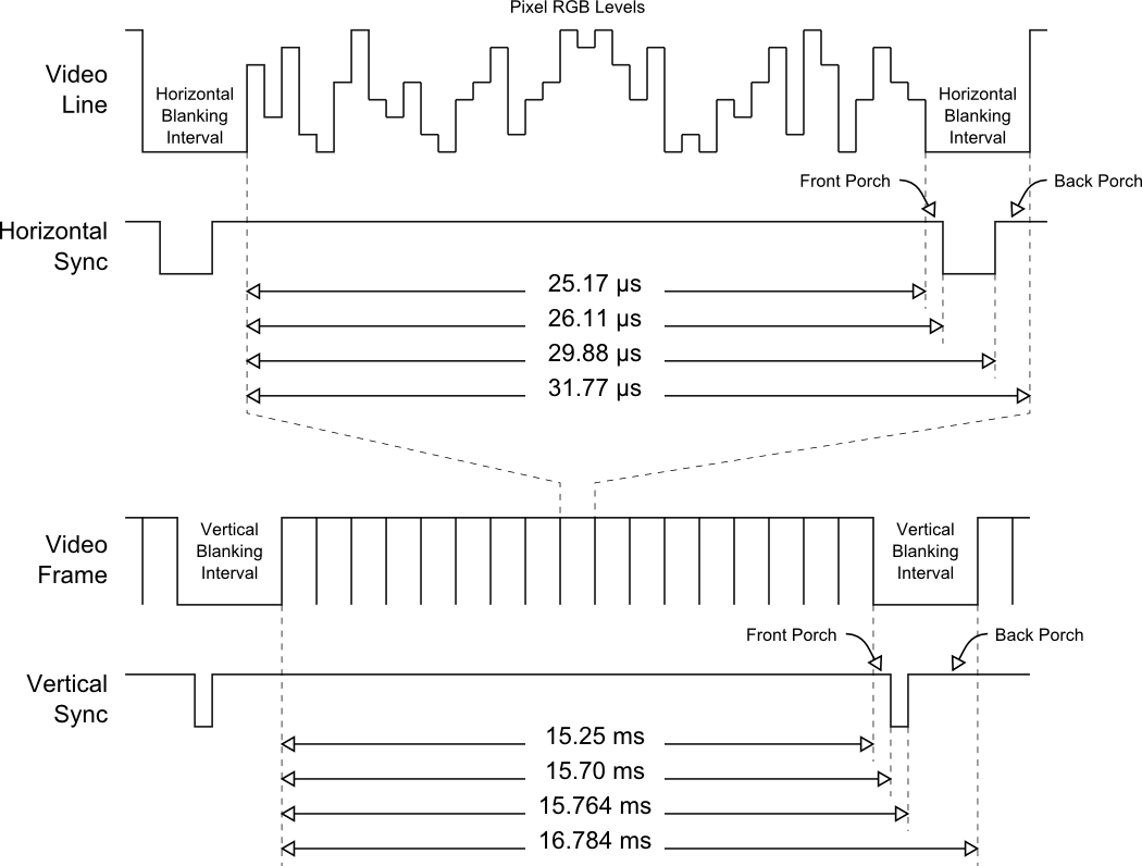
Timings vary from one VESA mode to another. I decided to use 1280x1024@60 mode, because that's resolution of my old LCD screen.
Top module
Inputs and outputs
I use 50 MHz external clock input and generate VESA signals:
module top (
  input  wire clk50,
  output wire vga_h_sync,
  output wire vga_v_sync,
  output reg  vga_R,
  output reg  vga_G,
  output reg  vga_B
);
I said before that R, G, B signals are analog... I drive them with digital output, so I can use only 8 colors.
Clock signals
Specification of 1280x1024@60 mode says that pixel frequency is 108.0 MHz. I used clock synthesis capabilities of my FPGA to get as close as possible to this frequency. By multiplying frequency times 13 it goes up to 650 MHz, than it is divided by 6 to go down to 108.333... MHz.
I also generate clock signal of the same frequency, but phase shifted by 180 degrees (clkps below). This will be useful for driving memory.
wire clk;
wire clkps;
clkdiv clkdiv
(
    .CLK_IN1(clk50),
    .CLK_OUT1(clk),
    .CLK_OUT2(clkps)
);
clkdiv above is an instance of a standard Spartan module that can be used for clock synthesis.
Synchronization
I use separate module to generate vga_h_sync and vga_v_sync outputs.
It also generates CounterX and CounterY data lines that tell which
pixel is being displayed. inDisplayArea and inPrefetchArea are helper signals and I will tell more about them later.
wire inDisplayArea;
wire inPrefetchArea;
wire [10:0] CounterX;
wire [10:0] CounterY;
sync_gen_1024x1080 syncgen
(
  .clk(clk),
  .vga_h_sync(vga_h_sync),
  .vga_v_sync(vga_v_sync),
  .inDisplayArea(inDisplayArea),
  .inPrefetchArea(inPrefetchArea),
  .prefetchCounterX(CounterX),
  .counterY(CounterY)
);
Memory
I use static memory built in on FPGA chip to store pixel data for current line and next line of the image.
my_ram image_ram (
  .clka(clkps), // input clka - has to be shifted from clock that generates data and address
  .ena(filler_read || gen_read), // input ena
  .addra(filler_read ? filler_addr : gen_raddr), // input [9 : 0] addra
  .douta(rdata), // output [15 : 0] douta
  .enb(gen_write || rst_write),
  .addrb(gen_write ? gen_waddr : rst_waddr),
  .dinb(gen_write ? gen_wdata : rst_wdata)
);
RGB signals
Current line is being read by filler module and sent to RGB signals.
wire        filler_read;
wire  [9:0] filler_addr;
wire [15:0] rdata;
assign filler_addr[9:8] = 0;
two_lines filler
(
    .clk(clk),
    .CounterX(CounterX),
    .CounterYparity(CounterY[0]),
    .inDisplayArea(inDisplayArea),
    .inPrefetchArea(inPrefetchArea),
    .read(filler_read),
    .addr(filler_addr[7:0]),
    .data(rdata),
    .image(image)
);

always @(posedge clk)
begin
  vga_R <= image & inDisplayArea; // one cycle of delay
  vga_G <= image & inDisplayArea; // (because we want no logic after reading signal from register to minimize output delay)
  vga_B <= image & inDisplayArea;
end
Image generation
Next line is computed from previous line by a process simulating cellular automaton when RGB data are not being sent (front porch, HSync and back porch).
wire gen_read;
wire gen_write;
wire [9:0]  gen_raddr;
wire [9:0]  gen_waddr;
wire [15:0] gen_wdata;
assign gen_raddr[9:8] = 0;
assign gen_waddr[9:8] = 0;
ca_gen gen
(
    .clk(clk),
    .start(CounterY < 11'd 1023 && CounterX == 11'd 1296),
    .direction(CounterY[0]),
    .read(gen_read),
    .raddr(gen_raddr[7:0]),
    .rdata(rdata),
    .write(gen_write),
    .waddr(gen_waddr[7:0]),
    .wdata(gen_wdata)
);
First line
There is separate process to initialize first line of the image. I initialize it with a single white pixel that moves from left to right.
wire rst_write;
wire [9:0]  rst_waddr;
wire [15:0] rst_wdata;
assign rst_waddr[9:8] = 0;
ca_gen0 reset (
    .clk(clk),
    .start(CounterY == 11'd 1023 && CounterX == 11'd 1296),
    .write(rst_write),
    .waddr(rst_waddr[7:0]),
    .wdata(rst_wdata)
);
Dive in
First line
Process that generates first line of the image is wired to memory
module by rst_write, rst_waddr and rst_wdata output lines.
As input lines it gets clock signal (clk) and start signal
that is activated at some point of time after last line
and before first line of the next frame.
module ca_gen0(
    input wire         clk,
    input wire         start,
    output reg         write,
    output reg  [7:0] waddr,
    output reg  [15:0] wdata
);
Its internal state consists of cycle (current internal clock cycle)
and position registers.
reg [10:0] position;
initial position = 0;

reg [7:0] cycle;
initial begin
    cycle = 8'd 160;
    wdata = 16'b0;
    waddr = 8'b0;
end
When start signal comes, cycle is initialized to 0 and position is incremented modulo 1280 (we have 1280 pixels in a line).
if (start)
begin
  wdata <= 16'b0;
  write <= 0;
  cycle <= 0;
  position <= (position + 1'b1) % 1280;
end
Before cycle reaches its final value of 160 (this is how many 16bit
memory writes are necessary to initialize used memory area) it
sets write to 1, increments cycle and writes some data to
wdata bus. cycle is being copied to waddr. All of this happens
at positive edge of a clock.
always @ ( posedge clk )
begin
    if (cycle != 8'd 160)
    begin
        if (cycle == position[10:4])
            wdata <= (1 << 15-position[3:0]);
        else
            wdata <= 16'b0;
        write <= 1;
        waddr <= cycle;
        cycle <= cycle + 1'b1;
    end
  ...
It is important to note that clock for memory module is phase shifted by 180 degrees. This gives some time for signals to stabilize before positive edge of memory clock signal comes.
Memory module
How much memory is needed? One line of the image has 1280 bits. We need to store previous and next line, because next line is calculated from previous line. This gives 2560 bits - not much. My Spartan-6 chip XC6SLX16 has 64 blocks of 9 Kibits (72 KiB in total).
To access memory I use BRAM_SDP_MACRO. It gives some abstraction over Spartan memory primitives. I set read width and write width to 16 bits. I select option to use output register. Documentation of this option says:
A value of 1 enables to the output registers to the RAM enabling quicker clock-to-out from the RAM at the expense of an added clock cycle of read latency. A value of 0 allows a read in one clock cycle but will have slower clock to out timing.
So I expect values to be present at the output after two clock cycles of RAM. Since RAM clock is phase shifted, I expect values after three main clock cycles.
Image generation
Module that generates next line of the image has similar structure to the module that generates first line of the image. There are two differences:
- It needs not only to write to memory, but also to read from the memory.
- It uses some combinatorial logic to generate next line from previous line.
Combinatorial logic is calculating next generation of cellular automaton state from previous generation. I've decided to do this in 16-bit blocks (memory width). Since state of a cell depends also on state of a neighboring cells I need 18 bits of an input for 16-bit output. I want screen to wrap around edge, so as value before first value in a line I take last value of a line.
So the sequence memory reads is:
- read last word of a line (to know value of last pixel in a line)
- read first word of a line
- read following words of a line till last one
We want last three memory reads to be available, so we store values in a shift register (which is filled through buffer2):
always @ ( posedge clk )
begin
    buffer0 <= buffer1[0];
    buffer1 <= buffer2;
end
The sequence of memory writes is simple: write from the first word till last one. But it needs to be delayed by right count of clock cycles (data must be available + one clock cycle for combinatorial logic of cellular automata).
Another thing is: we shouldn't write to the same memory location we will be reading from. Double buffering (of scanline pixels) is used. First buffer uses memory addresses 0-79, second uses words 80-159. This makes incrementing memory counter slightly complicated (I'm sure this could be simplified, e.g. by aligning memory ranges to power of 2):
function [7:0] increment_addr;
input [7:0] addr;
begin
    if (addr == 8'd 79)
        increment_addr = 8'd 0;
    else if (addr == 8'd 159)
        increment_addr = 8'd 80;
    else
        increment_addr = addr + 1'b1;
end
endfunction
To sum up, here is the pseudocode:
1. buffer[2] <= mem[rbegin+79]
2. buffer[2] <= mem[rbegin]
3. buffer[2] <= mem[rbegin+1]
4. left  = buffer[0][0]
   right = buffer[2][15]
   mem[wptr++] <= comb_ca(left, buffer[1], right)
   buffer[2] <= mem[rptr++]
... (as above)
84. mem[wptr] <= result
Filling lines
So far I've described how memory is filled with lines to be shown. But how is it sent to the screen?
From VGA synchronization module we are getting following information:
CounterX- current pixel in a line (pixel data is expected to be sent when it's 0-1279)CounterY- least significant bit of line number (remember? lines are double buffered...)inDisplayArea- are we in display area of a screen? - it's easier to calculate this in synchronization moduleinPrefetchArea- set to true some time beforeinDisplayAreais true to give time for memory read
The code is ugly, but it somehow works...
reg  [15:0] display_reg;
reg load_to_reg;

always @*
begin
    if (CounterYparity)
        addr[7:0] = CounterX[10:4] + 7'd 80;
    else
        addr[7:0] = CounterX[10:4];

    read         = inPrefetchArea && (CounterX[3:0] == 4'b0001); // on 0000 inDisplayArea is still false
    load_to_reg  = inPrefetchArea && (CounterX[3:0] == 4'b1111);
    image        = inDisplayArea && display_reg[15-CounterX[3:0]];
end

always @(posedge clk)
begin
    if (load_to_reg)
        display_reg <= data;
end
Most of the code above is combinatorial – not using clock input. Clock is used only in the part for storing data from memory into register. Would it be better to have registers for output signals?
For me this is both hard and important question when designing for FPGA. Maybe people designing digital electronics have some intuition about that. I don't have good intuition yet, but I see tradeoff:
- more combinatorial logic in one clock cycle — less clock cycles needed for processing;
- less combinatorial logic in one clock cycle — resulting circuit is less complicated, has smaller propagation delay, so faster clock can be used.
In this project clock is set to 108 MHz because of video mode requirements. If combinatorial logic is simple enough to have propagation delay less than 9.25 ns (~length of clock cycle) than I think it's the right level of complication.
Some of the output signals go to memory, which is clocked by signal shifted by 180 degrees. These signals have to propagate in half of clock cycle, so I think here is potential bottleneck. I'm pretty sure it's possible to calculate propagation delay of a signal with Xilinx tools, but I haven't tried that.
Synchronization
Finally, we go back to synchronization module. This is the heart of this project. It not only generates VESA synchronization signals (hsync, vsync), but also:
- address lines for current horizontal and vertical position;
- signals that tell if current position is in display area;
- signal that tells when to start prefetching line from memory.
Let's dive into the code.
We have separate block for current position (counterX and counterY).
wire counterXmaxed = (counterX == 11'd 1687);
wire counterYmaxed = (counterY == 11'd 1065);

always @(posedge clk)
begin
    if (counterXmaxed)
        counterX <= 0;
    else
        counterX <= counterX + 1'b1;

    if (counterXmaxed && counterYmaxed)
        counterY <= 0;
    else if (counterXmaxed && !counterYmaxed)
        counterY <= counterY + 1'b1;
end
Looks pretty straightforward. But counterX is actually private register.
It is set to be zero when horizontal synchronization starts.
This is convenient when calculating vga_h_sync output.
But outside of synchronization module it's more convenient
to start counting X position when display area starts or
some fixed time before (to have time to fetch pixel values from memory).
I have decided to start counting X position 16 pixels before
visible area. The name of the variable is prefetchCounterX.
`define FRONT_MARGIN 16
wire [10:0] xShift     = 112 + 248 - `FRONT_MARGIN;
always @(posedge clk)
begin
  // polarity of sync pulse is positive
  vga_h_sync <= counterX < 112;

  if (counterX == xShift)
    prefetchCounterX <= 0;
  else
    prefetchCounterX <= prefetchCounterX + 1'b1;
end
Why 112 + 248 - 16 above?
Horizontal:       width  start
 - visible area - 1280   0
 - front porch  - 48     1280
 - sync pulse   - 112    1328
 - back porch   - 248    1440
 - whole line   - 1688
I do no such tricks with Y position, so block for vga_v_sync is check for range of counterY:
always @(posedge vga_h_sync)
begin
    vga_v_sync <= counterY >= 11'd 1056 && counterY < 11'd 1059;
end
Finally, we have control signals that inform about being in display area and in prefetch area (to access pixel values at beginning of a line in advance).
always @(posedge clk)
begin
    inDisplayArea <= prefetchCounterX >= 11'd 15 && prefetchCounterX < 11'd 1295
                     && counterY < 11'd 1024;

   inPrefetchArea <= prefetchCounterX < 11'd 1280 && counterY < 11'd 1024;
end
Hardware setup
Hardware setup is very simple. Hsync and vsync are connected to matching VGA cable lines with 150 Ohm resistors (exact value doesn't really matter). R, G, B lines are connected to matching VGA lines with 270 Ohm resistors.
What's next
In this project I generate video output by calculating it on the fly line by line. For some real video output usually whole video frame is stored in memory. To do this I have to learn using SDRAM memory that is included on FPGA board I have.