- 018 How to stack
- 017 Brainf___ machine
- 016 Formal verification
- 015 How to count
- 014 Connecting FPGA to a computer
- 013 Binary numeric screen mode
- 012 VESA output by FPGA
- 011 Programming Xilinx Spartan 6
- 010 Learning basics of Verilog
- 009 Improvements in the blog engine
- 008 Migrating to AWS
- 007 LCD screens
- 006 Joule thief
- 005 Hall effect sensors
- 004 Constant acceleration revisited
- 003 Digital pendulum
- 002 Driving stepper motor
- 001 Play with forth and STM32
- 000 Hello world
Binary numeric screen mode
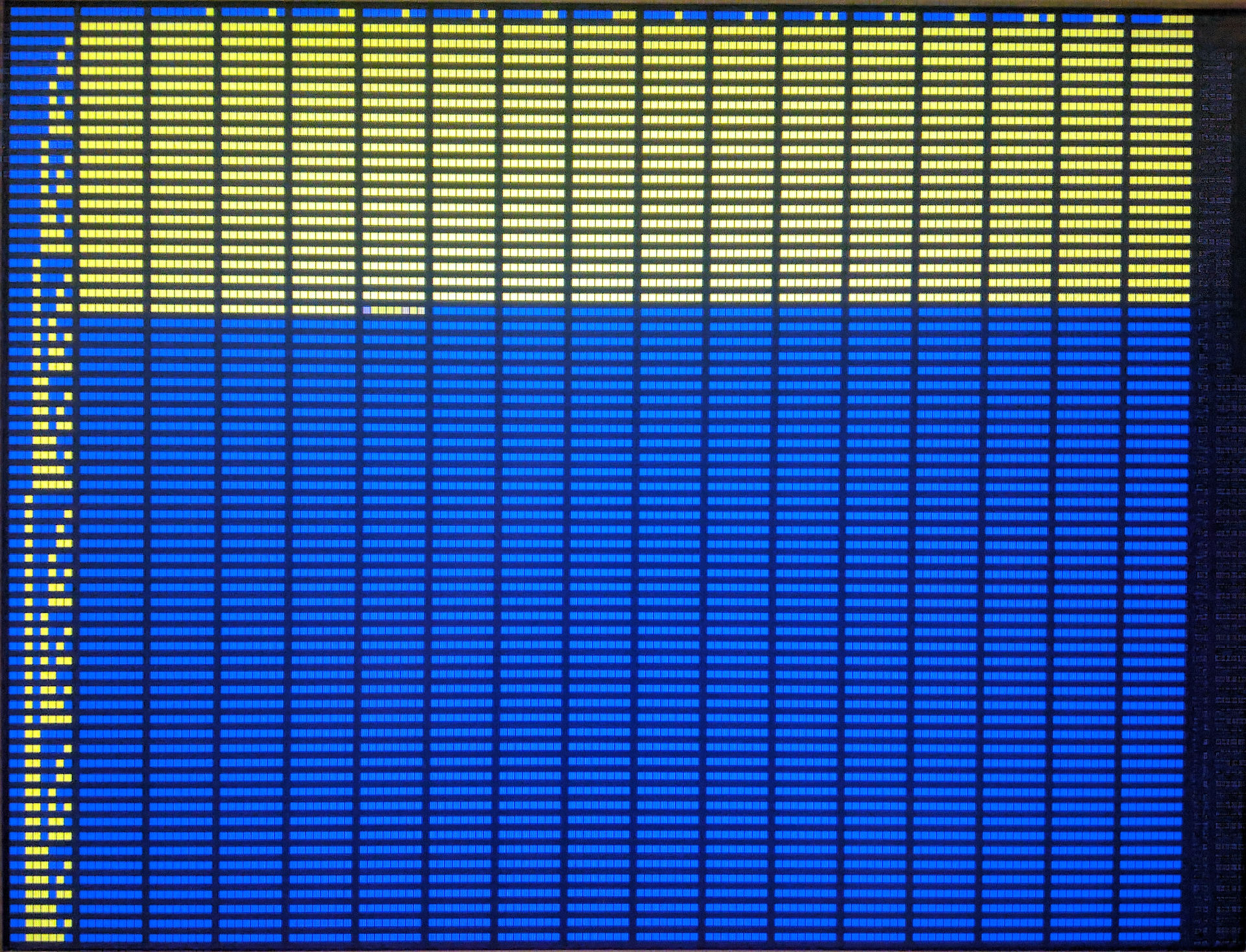
I always liked the looks of PDP-8 front panel.

You can stop processor at any moment, inspect registers and memory, single step it, etc. It can show contents of registers by turning on and of series of lamps (I think these are not LEDs...). Of course you have to read it binary.
Blinking LEDs when some condition is met is a well known method of FPGA debugging. It's not the best method, but a simple one. But why use some LEDs, when I have whole LCD screen connected?
Inspired by blinking lights of old computers I decided to create binary digital screen mode for my FPGA. The idea is to display contents of memory on a screen, grouped by bytes, with virtual lights. To make locating interesting bytes easier I also added row numbers and column numbers.
Top level view
This project is similar to previous one, so I was able to reuse some of its modules:
- a module for generating VGA synchronization signals
- a module for generating pixel clock frequency.
Let's look how modules are connected:
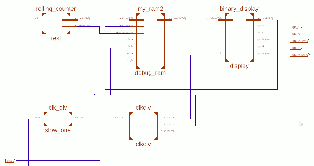
External clock signal goes to clkdiv module, where it is scaled up to 108 MHz,
because that frequency is needed by display module. Second output signal is also 108 MHz,
but it is phase shifted by 180°. This one goes to debug_ram module.
Third has the same frequency as input clock and goes to clock frequency divider
(slow_one module) where it is scaled down significantly. Slow clock signal
goes to the module being debugged (test) and also to debug_ram.
Did you notice that debug_ram gets two clock signals? This is dual port RAM
with two independent ports. Port A is used by test module. It puts some debug
data into the RAM. Port B is used by display module. It reads contents of
memory to display them on the screen. Port A and port B can have separate
clock signals.
This functionality is available in RAMB8BWER primitive of Spartan-6
and debug_ram is just a wrapper of a primitive from Spartan-6 library.
Having separate clock signals in two ports of RAM module is very useful.
It enables it to act as a buffer between logic being debugged and display
module that needs to be aligned with VGA pixel frequency.
Bumps along the road
Creating display module was quite straightforward. I reused VGA synchronization module from previous project and only needed some modulo arithmetic to calculate which memory address contents are just being sent trough VGA cable. That being said, there were some problems I had to solve.
Memory delay
In the first version that was able to read memory, values of memory cells were leaking to neighboring blocks. What's more interesting, when memory byte being read changes from 0 to 1, it requires one clock cycle more that when it changes from 1 to 0.
![]()
Static RAM that I use (RAMB8BWER) needs address to be stable some time before clock signal goes up. For details see Block RAM Timing Characteristics on page 31 of Spartan-6 FPGA Block RAM Resources.
Changing clock signal to phase shifted almost solved the problem. Now all values were "leaking" by one pixel. This was actually expected. Values need two clock cycles to become available in the output register of the memory.
I was prepared for that — I had a buffer that was delaying RGB signal already in the code — I only needed to delay "read memory" signal instead of RGB value. See this commit for details.
Using two clock signals
In my first attempt I connected external clock signal to both clkdiv module
(IP core from Xilinx) and to slow_one (my simple "divide frequency by counter" module).
I got an error that was hard for me to understand:
ERROR:Xst:2035 - Port
has illegal connections. This port is connected to an input buffer and other components.
But when I looked into code generated by IP core for clkdiv I noticed that
input clock in it first goes trough IBUFG.
The IBUFG is a dedicated input to the device which should be used to connect incoming clocks to the FPGA’s global clock routing resources. The IBUFG provides dedicated connections to the DCM, PLL, or BUFG resources. providing the minimum amount of clock delay and jitter to the device. The IBUFG input can only be driven by the global clock (GC) pins.
So I guess that this IBUFG element is placed near clock input pad on chip and that signal can either go trough it or bypass it, but not both.
I solved the problem by instructing clkdiv module to give third clock signal
at the output, that is identical to the input signal.
Result
As usually, source code is on GitHub.